

Secure Payment Guaranteed
Safe checkout with trusted global payment methods.
Why Choose Infinity Market Research?
At Infinity Market Research, we do not just deliver data - we deliver clarity, confidence, and competitive edge.
In a world driven by insights, we help businesses unlock the infinite potential of informed decisions.
Here is why global brands, startups, and decision-makers choose us:
Industry-Centric Expertise
With deep domain knowledge across sectors - from healthcare and technology to manufacturing and consumer goods - our team delivers insights that matter.
Custom Research, Not Cookie-Cutter Reports
Every business is unique, and so are its challenges. Thats why we tailor our research to your specific goals, offering solutions that are actionable, relevant, and reliable.
Data You Can Trust
Our research methodology is rigorous, transparent, and validated at every step. We believe in delivering not just numbers, but numbers that drive real impact.
Client-Centric Approach
Your success is our priority. From first contact to final delivery, our team is responsive, collaborative, and committed to your goals - because you are more than a client; you are a partner.
Recent Reports
Obesity Management Market
GLP-1 Receptor Agonist Market

Indium Phosphide Wafer Market
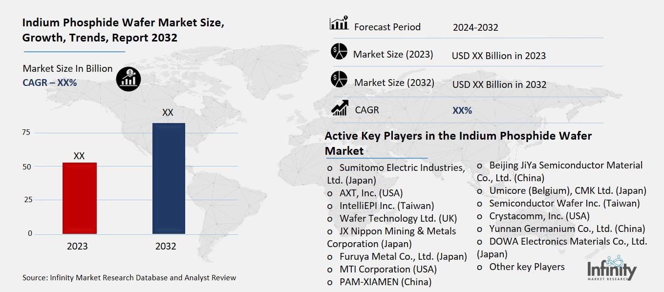
Indium Phosphide Wafer Market Global Industry Analysis and Forecast (2024-2032) By Diameter (8 Mm Or 2", 2 Mm Or 3", 100 Mm Or 4” and above) By End-User (Consumer Electronics, Telecommunications, Medical, Other end-user industry applications) and Region
Feb 2025
Semiconductor and Electronics
Pages: 138
ID: IMR1702
Indium Phosphide Wafer Market Synopsis
Indium Phosphide Wafer Market Size Was Valued at USD XX Billion in 2023, and is Projected to Reach USD XX Billion by 2032, Growing at a CAGR of XX% From 2024-2032.
The Indium Phosphide (InP) Wafer Market encompasses manufacturing and trading of wafers based on Indium Phosphide – a material that is appreciated for high electron velocity, high frequency and optical properties. These wafers play a major role in sophisticated applications such as high frequency telecommunications, lasers, photodetectors and sensors, including optoelectronic devices. The market is fueled by the increasing demand for broadband connectivity, 5G framework, and superior photonics; complemented by technology development and expanded application in defense, health care and automotive industries.
The global market for indium phosphide (InP) wafers is growing rapidly due to its indispensability in the development of improved semiconductor and optoelectronics devices. Being famed for high electron mobility, thermal conductivity, and optoelectronic features, InP wafers are mainstream for applications in telecommunication, aerospace and defense, health care, consumer electronics, etc. InP wafers are finding ever-increasing usage in optical communication systems due to the enhanced adoption of the 5G network, high bandwidth data applications, and their capability to produce efficient photonic devices like laser diodes, photodetectors, and modulators. Likewise, the growing uses of indium phosphide in high-frequency and high-power electronic devices now widely incorporated in computer chips such as transistors and multi-stage amplifier solidify its critical position in new technologies. Also, the market is increasing from PICs that use InP wafers to produce components that are small and possess low power consumption together with high speed.
Geographically, North America and Asia-Pacific are the lead the InP wafer market, owing to high technology development and well-established semiconductor sectors. Much of the research and development work is done in North America for applications in photonics and telecommunication through contributions by industry and governmental bodies. Another trend of the region’s development as an increase in the production of semiconductor components within the domestic industry strengthens its position in the market. On the flip side, Asia-Pacific is really doing great because it is the leader in consumer electronics manufacturers, rapid advancement of 5G networks, and rising Photonic technology investments. In the same manner, China, Japan and Korea markets are emerging to embrace the use of InP wafers in telecommunication, defense and medical facilities and other related departments. Europe is also a major factor for the market growth, owing to the consistent integration of photonic solutions across industrial processes encompassing industries like healthcare and energy.
Nevertheless, the market is not devoid of several challenges that might affect it in the future, so let us discuss them. The costs of production of InP wafers are considerably high due to the expensive raw materials required and in addition, the supply of the raw materials is limited thus posing a major challenge on scalability of production. These also make it possible for the end products produced to be expensive which may reduce market penetration especially in the low market segments. Moreover, the multistage operations in creating new products and the exclusive knowledge required in materializing such designs also come as a test to the manufacturers. Nevertheless, much remains encouraging, with rising market demand being fueled by advances in semiconductor technology and a growing partnership between firms and academic centers.
Further, the market is expected to continue on a growth path throughout the period as new applications and technologies come into play plus the niche but strong demand for Indium Phosphide wafer to support optoelectronics and photonics applications. Aspects in AI and machine learning, improving autonomous vehicles, and high-speed communication systems are predicted to present new markets for InP wafer in the future. Moreover, government plans to support domestic semiconductor industries and spur photonic technological progress will also remain the market growth main drivers. Considering the strategies of dealing with current challenges and engaging the new opportunities in question, the role of indium phosphide wafers as an essential part of the international and local semiconductor market is going to remain significant in the future.
Indium Phosphide Wafer Market Trend Analysis
Trend: InP Wafers Driving Advanced Telecommunications Infrastructure
The use of Indium Phosphide (InP) wafers is already defining the advance of tomorrow’s telecommunications networks especially in 5G network development and the subsequent.” Because of the high electron mobility, and excellent power handling capabilities, InP is a material of choice when it comes to preparing high end devices like transceivers, lasers and photodetectors. These components are fundamental in optical communication systems in fulfilling high speed data transfer in increasing global telecommunication networks. Increased requirement of higher bandwidth and low latency in new applications like healthcare, autonomous vehicles and IoT is adding to the adoption of InP based technologies in telecom segment.
At the same time, the volume of consumption of InP wafers increases due to the growing popularity of data centers and cloud solutions. These facilities entail highly efficient and dependable system of optical communication to meet the escalating traffic. InP based devices allow for higher transmission rates for fewer watts thus meeting the fundamental performance and energy budget of modern data centers. Growth in cloud computing solutions and big data analytics solutions creates new demand for InP wafers as a core material in optical networking solutions, encouraging growth and development in the market.
Drivers: Critical Role of Indium Phosphide in Optoelectronic Devices
Indium Phosphide (InP) substrate wafer is widely used for fabrication of high-performance optoelectronic devices including photodetectors, lasers and modulators utilized in the optical fiber communication system. Due to the development of the Internet services, further evolution of the launching 5G technologies, and the inclination toward cloud solutions, there is a high demand for the high-speed data transmission systems. Such networks need parts that at high data rates operate effectively but consume minimal power and InP wafers serve perfectly. InP superior electron mobility and direct bandgap characteristics, make it possible to fabricate devices that provide greater efficiency in optical communications and thus deepening its integration into the telecommunications sector.
Due to the booming demands of data centric technologies like 5G, cloud computing the sophisticated semiconductors with higher capacity are in requirement. Of all the available materials, Indium Phosphide has proved to be the most suitable to allow circuits to operate at high frequency and high power levels as can be desired. Growing with these technologies, the need for all InP-based components especially in high-speed data applications such as fibre optics and integrated photonics will propel the market forward. The constant drive towards improving efficiency and data rates in today’s telecommunication and many other fields guarantees essentiality of InP wafers and drives their more extensive utilization across numerous fields.
Restraints: High Production Costs of InP Wafers
Lack of economies of scale is another problem facing Indium Phosphide (InP) wafers due to the costly process when producing wafers. The fabrication of InP wafers entails the use of complex tools and high level technology hence the development of costs. These high costs put the material in a challenge of finding good market due to the limitations it has in terms of use this restricted the use of this material to only the telecommunication and optoelectronics industries. This restricts its application on large markets, because the cost of InP wafers may outweigh the advantages of the material for such budget-sensitive applications that are not likely to fully utilise the capabilities of the component.
However, the price issue due to the high cost of InP wafers has been a formidable challenge to smaller firms and new entrant in the market. Small and medium-sized enterprises are revenue restricted from further investing in sophisticated equipment and personnel to design InP material-products. Consequently, these companies may fail to integrate InP wafers in their products or develop technologies that can challenge those of well-established counterpart companies. On a cost front, this acts as a disadvantage in the advancement and ability of fresh innovations among the numerous small players in the market that in a way constrains the growth of the overall InP wafer market .
Opportunities: Increasing Adoption of InP-Based Devices in Telecommunications
The potential, which is one of the biggest Indium Phosphide (InP) wafer market drivers, relates to the use of InP-based devices in telecommunications industry especially in high frequency fibre-optic application. Growing international demand for high-frequency communication networks has created significant need for InP wafers to support production of other devices like laser diodes, amplifiers, and modulators. These components are critical in carrying high bandwidth signals and therefore InP wafers are crucial in optimizing the telecommunication. These wafers are forecasted to have a strong increase in demand in line with the speedy deployment of new 5G networks that rely on efficient and high-speed networks, low latency, materials that are advanced.
The demands for 5G and future optic communication systems which could be installed in various products offer a good market opportunity for manufacturers who supply InP wafers. Since mobile and fixed telecommunication operators seek to offer consumers and businesses higher bandwidths and improved connectivity, this presents a continuous requirement for higher-performing parts. InP based devices are on one hand perfectly suitable to meet these challenges thanks to the ability to process high frequency signals with very good performance. Therefore, manufacturers are set to strongly associate the telecommunications’ category for a long-term growth, where InP wafers are positioned to play a crucial role for future communication solutions.
Indium Phosphide Wafer Market Segment Analysis
Indium Phosphide Wafer Market Segmented on the basis of By Diameter, By End-User.
By Diameter
o 8 Mm Or 2"
o 2 Mm Or 3"
o 100 Mm Or 4” and above
By End-User
o Consumer Electronics
o Telecommunications
o Medical
o Other end-user industry applications
By Region
o North America (U.S., Canada, Mexico)
o Eastern Europe (Bulgaria, The Czech Republic, Hungary, Poland, Romania, Rest of Eastern Europe)
o Western Europe (Germany, UK, France, Netherlands, Italy, Russia, Spain, Rest of Western Europe)
o Asia Pacific (China, India, Japan, South Korea, Malaysia, Thailand, Vietnam, The Philippines, Australia, New-Zealand, Rest of APAC)
o Middle East & Africa (Turkey, Bahrain, Kuwait, Saudi Arabia, Qatar, UAE, Israel, South Africa)
o South America (Brazil, Argentina, Rest of SA)
By Diameter, 8 Mm Or 2" segment is expected to dominate the market during the forecast period
The segment for components with a diameter of 8 mm, or approximately 2 inches, plays a crucial role in industries where space constraints and precision are essential. In the consumer electronics sector, this diameter is highly sought after for its ability to maintain the compactness and functionality of modern devices. Smartphones, cameras, and wearable technology benefit from such components as they allow for miniaturization without sacrificing performance. Additionally, connectors, cables, and micro-components with an 8 mm diameter are integral to ensuring seamless integration in consumer devices. As devices become slimmer and more powerful, the demand for such compact components continues to rise.
In telecommunications, where space and performance are at a premium, 8 mm components are particularly valuable. These components are used in microelectronics, connectors, and high-density cables that support faster data transmission and improved connectivity. As telecommunications technologies evolve, especially with the ongoing push for 5G networks, the need for these small yet powerful components is increasing. The market for 8 mm diameter products is expected to grow as industries continue to demand smaller, more efficient components capable of delivering high performance in increasingly space-constrained environments. The miniaturization of electronics in these sectors ensures that 8 mm components will remain a key player in both consumer electronics and telecommunications industries.
By End-User, Consumer Electronics segment expected to held the largest share
The consumer electronics sector is one of the most significant end-users for components across a wide range of diameters, with applications spanning from small, compact devices to larger home appliances. As the demand for sleek, lightweight, and more efficient products grows, the need for miniaturized components becomes increasingly critical. Components with diameters such as 8 mm and 2 mm are particularly essential for devices like smartphones, tablets, laptops, wearables, and home appliances. These smaller components enable manufacturers to create thinner and more feature-packed devices without compromising on performance. The ongoing trend toward smaller form factors, combined with the growing emphasis on portability, ensures that components in these diameter ranges will continue to be in high demand within the consumer electronics market.
As consumer electronics evolve, particularly with advancements like foldable screens, 5G connectivity, and enhanced multimedia capabilities, the need for high-performance components will only increase. The shift towards more powerful and energy-efficient devices drives a continuous requirement for specialized components that support these innovations. For example, smaller and more efficient connectors, sensors, and chips in the 8 mm and 2 mm ranges are becoming critical in ensuring seamless device performance, enhanced connectivity, and extended battery life. This rapid technological development, particularly in next-generation devices, positions the consumer electronics sector as a primary driver of growth for components across all diameter sizes, underscoring the importance of these miniaturized yet high-performance parts.
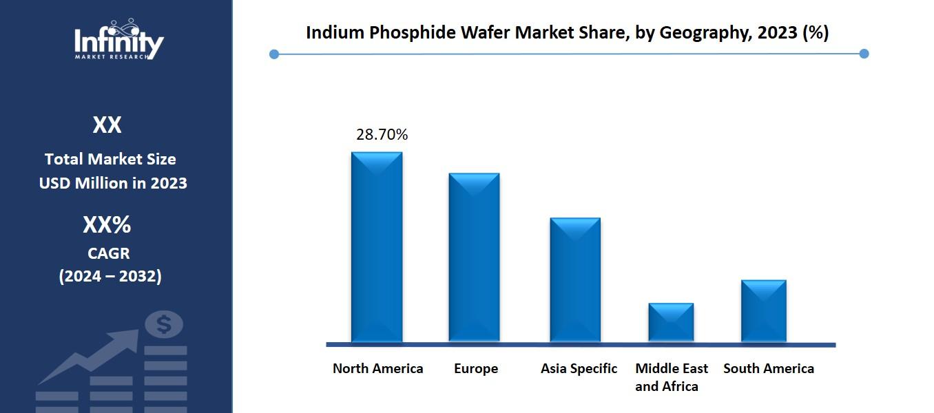
Indium Phosphide Wafer Market Regional Insights
North America is Expected to Dominate the Market Over the Forecast period
Indium Phosphide (InP) wafer also has its largest demand from North America, due to the position of the United States and Canada as the major semiconductor production and advanced high-tech industries. The situation in this respect is that the region is experiencing fast progress in the field of telecommunications, mainly with the 5G network that relies so much on sophisticated semiconductor material such as InP. In addition to this, the rise in data centers and fiber optic communication systems increases the need for InP wafers used in high speed data communication system and optical communication. The progress in these sectors is enhancing the setup favorable for innovation, where InP based devices are regime for upcoming digital networking.
The major growth contributors for the InP wafer market include Telecommunication, Defense and Aerospace industries mainly operating in North America . These sectors need special components as InP wafers integrated for applications like satellite telecommunication, radar systems and many more. The United States occupies a special place given the high levels of R & D invested in the country and the growing popularity of InP based device throughout the sectors of high technologies. This growing adoption along with the continuous increase in R & D North America is seen as a key player in the development of the Indium Phosphide Wafer Market.
Indium Phosphide Wafer Market Share, by Geography, 2023 (%)
Active Key Players in the Indium Phosphide Wafer Market
o Sumitomo Electric Industries, Ltd. (Japan)
o AXT, Inc. (USA)
o IntelliEPI Inc. (Taiwan)
o Wafer Technology Ltd. (UK)
o JX Nippon Mining & Metals Corporation (Japan)
o Furuya Metal Co., Ltd. (Japan)
o MTI Corporation (USA)
o PAM-XIAMEN (China)
o Beijing JiYa Semiconductor Material Co., Ltd. (China)
o Umicore (Belgium), CMK Ltd. (Japan)
o Semiconductor Wafer Inc. (Taiwan)
o Crystacomm, Inc. (USA)
o Yunnan Germanium Co., Ltd. (China)
o DOWA Electronics Materials Co., Ltd. (Japan)
o Other key Players
Global Indium Phosphide Wafer Market Scope
|
Global Indium Phosphide Wafer Market | |||
|
Base Year: |
2023 |
Forecast Period: |
2024-2032 |
|
Historical Data: |
2017 to 2023 |
Market Size in 2023: |
USD XX Billion |
|
Forecast Period 2024-32 CAGR: |
XX% |
Market Size in 2032: |
USD XX Billion |
|
|
By Diameter |
· 8 Mm Or 2" · 2 Mm Or 3" · 100 Mm Or 4” and above | |
|
By End-User |
· Consumer Electronics · Telecommunications · Medical · Other end-user industry applications | ||
|
By Region |
· North America (U.S., Canada, Mexico) · Eastern Europe (Bulgaria, The Czech Republic, Hungary, Poland, Romania, Rest of Eastern Europe) · Western Europe (Germany, UK, France, Netherlands, Italy, Russia, Spain, Rest of Western Europe) · Asia Pacific (China, India, Japan, South Korea, Malaysia, Thailand, Vietnam, The Philippines, Australia, New-Zealand, Rest of APAC) · Middle East & Africa (Turkey, Bahrain, Kuwait, Saudi Arabia, Qatar, UAE, Israel, South Africa) · South America (Brazil, Argentina, Rest of SA) | ||
|
Key Market Drivers: |
· Critical Role of Indium Phosphide in Optoelectronic Devices | ||
|
Key Market Restraints: |
· High Production Costs of InP Wafers | ||
|
Key Opportunities: |
· Increasing Adoption of InP-Based Devices in Telecommunications | ||
|
Companies Covered in the report: |
· Sumitomo Electric Industries, Ltd. (Japan), AXT, Inc. (USA), IntelliEPI Inc. (Taiwan), Wafer Technology Ltd. (UK), JX Nippon Mining & Metals Corporation (Japan), Furuya Metal Co., Ltd. (Japan), MTI Corporation (USA), PAM-XIAMEN (China), Beijing JiYa Semiconductor Material Co., Ltd. (China), Umicore (Belgium), CMK Ltd. (Japan), Semiconductor Wafer Inc. (Taiwan), Crystacomm, Inc. (USA), Yunnan Germanium Co., Ltd. (China), DOWA Electronics Materials Co., Ltd. (Japan) and Other Major Players. | ||
Frequently Asked Questions
1. What would be the forecast period in the Indium Phosphide Wafer Market research report?
Answer: The forecast period in the Market research report is 2024-2032.
2. Who are the key players in the Indium Phosphide Wafer Market?
Answer: Sumitomo Electric Industries, Ltd. (Japan), AXT, Inc. (USA), IntelliEPI Inc. (Taiwan), Wafer Technology Ltd. (UK), JX Nippon Mining & Metals Corporation (Japan), Furuya Metal Co., Ltd. (Japan), MTI Corporation (USA), PAM-XIAMEN (China), Beijing JiYa Semiconductor Material Co., Ltd. (China), Umicore (Belgium), CMK Ltd. (Japan), Semiconductor Wafer Inc. (Taiwan), Crystacomm, Inc. (USA), Yunnan Germanium Co., Ltd. (China), DOWA Electronics Materials Co., Ltd. (Japan) and Other Major Players.
3. What are the segments of the Indium Phosphide Wafer Market?
Answer: The Indium Phosphide Wafer Market is segmented into By Diameter, By End-User and region. By Diameter, the market is categorized into 8 Mm Or 2", 2 Mm Or 3", 100 Mm Or 4” and above. By End-User, the market is categorized into Consumer Electronics, Telecommunications, Medical, Other end-user industry applications. By region, it is analyzed across North America (U.S.; Canada; Mexico), Eastern Europe (Bulgaria; The Czech Republic; Hungary; Poland; Romania; Rest of Eastern Europe), Western Europe (Germany; UK; France; Netherlands; Italy; Russia; Spain; Rest of Western Europe), Asia-Pacific (China; India; Japan; Southeast Asia, etc.), South America (Brazil; Argentina, etc.), Middle East & Africa (Saudi Arabia; South Africa, etc.).
4. What is the Indium Phosphide Wafer Market?
Answer: The Indium Phosphide (InP) Wafer Market encompasses manufacturing and trading of wafers based on Indium Phosphide a material that is appreciated for high electron velocity, high frequency and optical properties. These wafers play a major role in sophisticated applications such as high frequency telecommunications, lasers, photodetectors and sensors, including optoelectronic devices. The market is fueled by the increasing demand for broadband connectivity, 5G framework, and superior photonics; complemented by technology development and expanded application in defense, health care and automotive industries.
Secure Payment Guaranteed
Safe checkout with trusted global payment methods.
Why Choose Infinity Market Research?
- Accurate & Verified Data:Our insights are trusted by global brands and Fortune 500 companies.
- Complete Transparency:No hidden fees, locked content, or misleading claims - ever.
- 24/7 Analyst Support:Our expert team is always available to help you make smarter decisions.
- Instant Savings:Enjoy a flat $1000 OFF on every report.
- Fast & Reliable Delivery:Get your report delivered within 5 working days, guaranteed.
- Tailored Insights:Customized research that fits your industry and specific goals.
Need custom data?
Get tailored segments, regions, competitors, or analyst support for this report.
